Can an ADC Be Just a Random Number Generator?
2025-10-22
How good is an ADC? This question is not asking about how many bits of resolution it has; it may come as a surprise to know that a 16-bit ADC will not always give 16-bits of useful information! "A lot of 16-bit ADCs really operate as 7-bit ADCs and 9-bit random number generators," says Mike Stone in “Choosing an ADC”. This article shows how to determine if an ADC is generating more random numbers than useful ones, along with a few simple ways to reduce the randomness.
Consider a simplified setup: an ADC measuring the voltage on a photoresistor. If the 12-bit ADC in Figure 1 (with VFS = 3.3 V) reports a value of 2048, then does that mean the voltage on the photoresistor is 1.65 V?
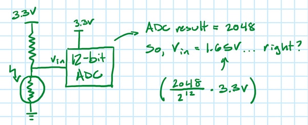 Figure 1: Simplified ADC setup for measuring a photoresistor voltage. (Image source: Nathan Jones)
No, not really! To demonstrate, take a second sample, then a third, and, in fact, take 100,000 samples and plot the results. What will be seen is a distribution of ADC values (Figure 2); if nothing has changed in the setup, then any one of these could be the true voltage on the photoresistor, with the likeliest candidate being the average value of all those samples.
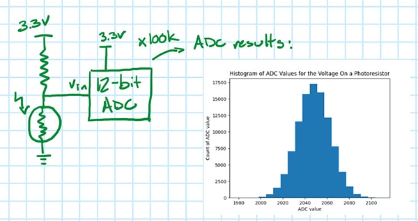 Figure 2: The insert shows the histogram of ADC values for 100,000 samples of photoresistor voltage. (Image source: Nathan Jones)
That brings up another question. Could some of that variation be actual variations in the input signal? Yes, it could. To test this, the resistive divider will be swapped out for a voltage reference (Figure 3) with a known noise level and the experiment repeated.
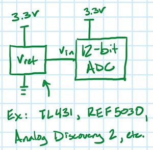 Figure 3: New test setup with a voltage reference in place of the resistive divider. (Image source: Nathan Jones)
Ideally the voltage reference used should have a noise level which is less than 1/3 of the noise level expected in the ADC (e.g., if the ADC is expected to have ±1 LSB of noise [which would be ±0.8 mV using the ADC in the example above], then ideally the voltage reference should have a noise level of less than 0.27 mVpp); if it does, then it is expected that all of the measured noise must be coming from the ADC, based on the fact that uncorrelated noise adds in quadrature (Equation 1).
 [1]
[1]
If NoiseVref=NoiseADC/3 then Noisetotal=1.054 × NoiseADC. This would mean that the voltage reference contributes just 5.4% of the total noise, a negligible amount. If it turns out that the voltage reference is noisier than 1/3 of the noise from the ADC, just remember to subtract its contribution from the measured standard deviation (see Equation 2).
 [2]
[2]
How to know a voltage source’s noise level
The easiest way is to find it on the datasheet. Here’s an example from the datasheet for the Texas Instruments REF5030, showing that it has a noise level of 9 μVpp.
 Figure 4: Excerpt from the REF5030 datasheet showing the output voltage noise specification. (Image source: Texas Instruments)
If the datasheet doesn’t list a noise level (or to just verify its value), just measure it with an oscilloscope, though the noise floor of the oscilloscope needs to be known first. This can be done by connecting one of the oscilloscope inputs to ground and measuring the RMS value of the variations in the signal seen. Figure 5 shows the result of doing this with an Analog Discovery 2 (AD2), demonstrating that the RMS noise is about 0.9 mV. Interesting, this value decreases (down into the µV range) if the time base is increased beyond 8 µs/div, presumably because the AD2 is using oversampling and decimation to increase its effective resolution.
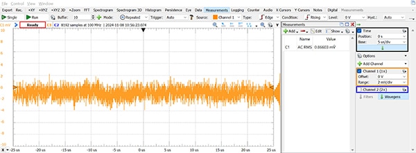 Figure 5: Noise floor level plot of the Analog Discovery 2 oscilloscope. (Image source: Nathan Jones)
When the voltage source is measured, any variations in the oscilloscope signal are the result of the combined noise in both the voltage source and the oscilloscope. As long as those noise sources are uncorrelated (they are), then Noisemeasured=√(Noise²Scope+Noise²Vref) and NoiseVref=√(Noise²Measured-Noise²Scope), like above. When a 2 VDC signal that was generated by the AD2 was measured, the noise was determined to be 1.2 mV (Figure 6).
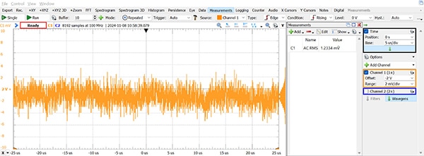 Figure 6: This plot of a 2 VDC signal indicates that the oscilloscope noise was 1.2 mV. (Image source: Nathan Jones)
This would indicate that the signal generator on the AD2 also has a noise level of about 0.9 mV. This is low enough to test a 10-bit ADC (0.9 mV is just less than 1/3 of an LSB for a 10-bit ADC with 3.3 V full-scale reading); for any higher-resolution ADCs, this noise would have to be accounted for in the measurements.
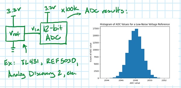
Figure 7: The insert shows the new histogram of ADC values for 100,000 samples of photoresistor voltage with the voltage reference. (Image source: Nathan Jones)
That’s much better! Notice now how the second histogram (Figure 7) only goes out to 2052 on the x-axis (the distribution on that graph [Figure 8] has a standard deviation of 1 LSB), while the first graph went out to 2100 (it had a standard deviation of 15 LSBs). This is called a DC Histogram test for an ADC and the standard deviation effectively indicates how much noise there is in the ADC: anytime a value is measured with the ADC, there’s only a 68% chance that the true value on the analog pin is actually within ±1 standard deviation of that value, but there’s a 99.7% chance that the true value is within ±3 standard deviations of that value.
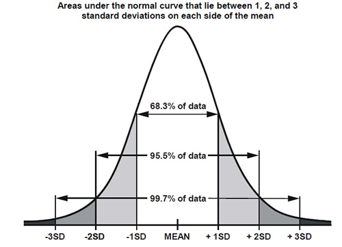 Figure 8: Distribution curve with standard of deviations. (Image source: https://i.sstatic.net/jkMDV.png)
Converting this standard deviation from LSBs to volts results in the input-referred noise for the ADC (Equation 3).
![Input - referred noise [V_RMS ]=(σ∙V_FS)/2^N Equation 3](http://sc-c.digikeyassets.com/-/media/Images/Article%20Library/TechZone%20Articles/2025/October/Can%20an%20ADC%20Be%20Just%20a%20Random%20Number%20Generator/article-2025october-can-an-adc-be-just-equation3.jpg?la=en&ts=6126a5a1-ecae-4e79-bfb0-97e98cce83fa) [3]
[3]
If the ADC has such little noise that all ADC codes do fall into a single bin, try lowering the ADC reference voltage. The noise level will stay the same but will take up more ADC codes than before, allowing a proper value for the input-referred noise to be found.
The effective resolution and the noise-free code resolution (NFCR) of an ADC represent the extent to which this noise limits the ADC resolution, which are calculated by dividing the full range of ADC codes into bins that are only as wide as either one (Equation 4) or 6.6 standard deviations (Equation 5).
 [4]
[4]
 [5]
[5]
Essentially, there are fewer actual bits in the result because there’s an increasing chance that the last few bits in the ADC result are wrong or noisy.
A slightly more straightforward version of the DC Histogram test involves simply grounding the input of the ADC and then creating a histogram (Figure 9) of the ADC results, as was done for the oscilloscope.
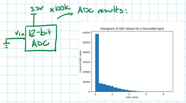 Figure 9: The insert shows the histogram of the ADC output voltage samples with the input grounded. (Image source: Nathan Jones)
The standard deviation of this histogram is also a measure of the ADC noise (minus any contributions from noise in the ADC reference voltage, which won’t affect readings of 0 V), but it’s optimistically low. The ADC probably reports values less than 0 V as just 0, so only half of the true noise distribution is being seen. In this case, the ADC noise could be approximated if it is assumed that the distribution was symmetric about its average value, changing enough of the median values to negative numbers so that the distribution became symmetric and then calculating the standard deviation of that (Figure 10).
 Figure 10: Mirroring of the Figure 9 histogram to approximate the ADC noise. (Image source: Nathan Jones)
Okay, so what can be done about all this noise? If the resolution of the ADC is still within the project requirements (lucky!), then just keep in mind that every ADC measurement comes with some uncertainty:
- When comparing two ADC values, treat them as being equivalent only if they’re within 6.6 σ of each other (to be 99.7% confident in the comparison) or if they’re within σ of each other (to be only 68% confident).
- When comparing an ADC value to a threshold, add some hysteresis to the threshold comparison (like a thermostat does) to avoid the embedded system from re-triggering above and below that threshold just based on noise.
If it turns out that the ADC doesn’t meet the project requirements anymore, there are a few simple things to try to improve its performance. On the hardware side, these include:
- Using a lower-noise reference (such as the Texas Instruments REF5030 or the EVVO TL431) for AVCC and AREF
- Ensuring minimal crosstalk between analog and digital signals on the PCB
- Turning off the CPU during ADC conversions (if the MCU supports it), to reduce digital noise
On the software side, the input signal can be oversampled (i.e., take the average of N samples) to reduce noise, though this will clearly reduce the maximum sampling rate. (In fact, a technique called “oversampling and decimation” could be used to increase the resolution of the ADC by an amount related to the number of times the input is oversampled!)
Assume the standard deviation of a DC Histogram test for the initial setup is 1 LSB. If the ADC reads 2048, now does that mean (there’s a 68% chance) the true value is 1.650±0.008 V (Figure 11)?
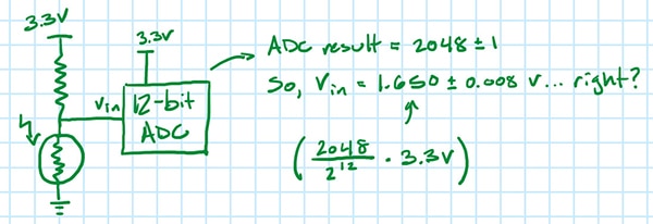 Figure 11: Assuming the standard of deviation of the Figure 1 setup is 1 LSB and the ADC output is 2048, is the true input voltage 1.650±0.008 V? (Image source: Nathan Jones)
Closer, but still no! That’s because all ADCs will struggle with measuring a rapidly changing input signal at some frequency, resulting in imprecise measurements (i.e., noise). Surprisingly, the frequency at which that occurs may be well below the maximum sampling rate for the ADC! This means that a 12-bit ADC with a sampling rate of 1 MSPS (mega-samples per second) may not actually have 12-bits of resolution for input signals near 500 kHz; the resolution of that ADC may fall to 6-bits or lower when the input signal frequency is that high. If trying to measure a signal on the photoresistor that’s above 10 Hz, the ADC may not actually have 12-bits of resolution.
To determine how well the resolution of the ADC holds up with higher input frequencies, send in a known-good signal (this time, a sine wave) and measure how closely the ADC values match that known-good signal (Figure 12). (Is the sine wave “good enough”? That will be discussed after the procedure for performing the test is revealed; it will make more sense that way.)
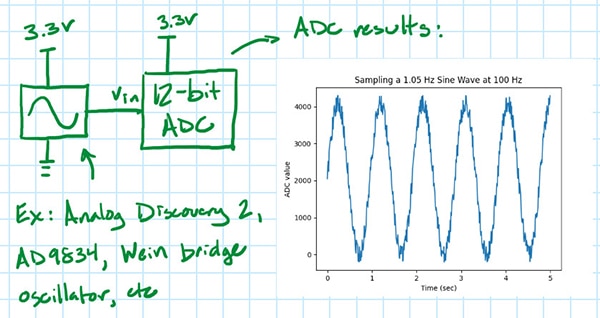 Figure 12: Test setup with a known-good sine wave input. (Image source: Nathan Jones)
For the sine wave, a function generator can be used (like the ones found on many USB oscilloscopes), a DDS chip (like Analog Devices’ AD9834), or a custom sine wave generator can be assembled (based on a Wien bridge oscillator or by using a MAX7400 from Analog Devices to lowpass filter a square wave, for example). It is important to note that only input frequencies for this test that are not integer sub-multiples of the sampling frequency should ever be used (e.g., don’t use an input frequency of 1 kHz if the sample rate is 100 kHz). This is to avoid erroneously sampling the sine wave in the same locations on every cycle. Additionally, to maximally stress the ADC, set the input sine wave’s amplitude to the largest value that doesn’t “clip” the output (e.g., something slightly less than 1.65 V for the ADC in the examples above).
After collecting the ADC results, the data is fit to a sine wave to calculate the residual error. The sine wave fit can be performed with almost any amount of data, but to get the best results, there has to be at least five full periods of the input sine wave. It is likely that the sine-fitting algorithm will have to be initialized by giving it initial guesses for the amplitude, frequency, phase shift, and offset (Figure 13).
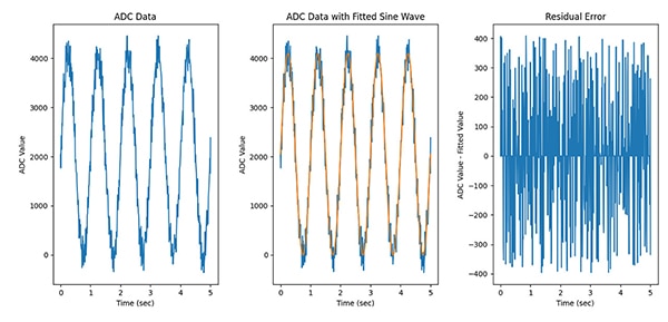 Figure 13: Using a sine wave fitting algorithm, the residual error can be determined. (Image source: Nathan Jones)
This test is called the sine wave fit test for an ADC, and the RMS value of the residual error is a measure of how noisy the ADC is at that specific input frequency. At lower frequencies, the RMS noise should match the input-referred noise from the DC histogram test, but at higher frequencies it will almost certainly degrade as a result of those frequency-dependent noise sources mentioned above.
The RMS noise value from the sine wave fit test can be used to calculate the effective number of bits (ENOB) of the ADC (Equation 6), which is the number of bits of an ideal ADC whose only noise source, quantization noise, has the same RMS value as the noise in the ADC.
 [6]
[6]
This value is specific to the frequency of the input signal that was used. To get a more complete picture of the ADC, this test should be repeated at frequencies all the way up to the highest input signal of interest, or up to half of the maximum sampling rate. It may be found that the noise goes way up (and the ENOB way down!) at frequencies well below half of the maximum sampling rate! For example, that exact series of tests were performed on the ADC in an STMicroelectronics STM32F042K6 and plotted the results (Figure 14).
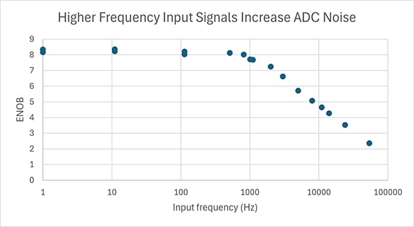 Figure 14: Frequency noise test for an ADC in an STM32F042K6 microcontroller. (Image source: Nathan Jones)
Even though the ADC on the STM32F042K6 microcontroller can sample at 1 MHz, the resolution falls off above 1 kHz; if the intent was to measure a 10 kHz signal with this ADC, there would only be about 5 bits of resolution at that point! (Notice, also, that the maximum ENOB is around 8.3; this is due to ~10 LSBs of noise even at DC, which reduce the effective resolution of the ADC from 12 bits to around 8.7 bits right off the bat. These tests were conducted on an unmodified STMicroelectronics Nucleo-F042 development board; results would be much better if any of the techniques mentioned above are used [“Okay, so what can be done about all this noise?”].)
How to know a sine wave’s noise level
As with the voltage reference, if the noise level of the sine wave is a priori (i.e., if it’s not available on a datasheet), then there is a need to measure it with an oscilloscope. The use of the sine wave fitting technique discussed earlier can characterize the noise from the sine wave generator.
- First, determine the noise floor of the oscilloscope by connecting its input to ground and calculating the RMS value of the output (as described earlier in the “How to know a voltage source’s noise level” section).
- Then, measure the output from the sine wave generator, fit the results to a perfect sine wave, and calculate the RMS value of the residuals. Then use Equation 2 to determine the noise of the sine wave generator (using the oscilloscope’s noise floor as an approximation of its AC noise).
- Ensuring that the output impedance of the device that’s connected to the analog pin is very low, possibly inserting an op-amp for buffering
- Adjusting the ADC clock or its sample/hold time to be as fast as possible, while still giving the internal capacitor enough time to charge
- Using a low-jitter ADC clock source and configuring the system to take ADC samples at regular intervals
- Characterizing the Raspberry Pi Pico ADC
- Understanding Data Converters (Texas Instruments)
- Understand SINAD, ENOB, SNR, THD, THD + N, and SFDR so You Don't Get Lost in the Noise Floor (Analog Devices)
- The Good, the Bad, and the Ugly Aspects of ADC Input Noise--Is No Noise Good Noise? (Analog Devices)
- Getting the most out of the SAM D21's ADC (Thea Codes)
- "Analog-to-Digital Converter Testing" (Kent Lundberg)
- Dynamic Tests For A/D Converter Performance (Texas Instruments)
- How to optimize the ADC accuracy in the STM32 MCUs (STM)
- Enhancing ADC resolution by oversampling (Atmel)
- Fundamentals of Precision ADC Noise Analysis (Texas Instruments)
- ADC Gain and Offset Error Calibration on ARM® Cortex®-M0+ Based MCUs (Microchip)
- Sine wave generation via low-pass filtering a square wave
- Understanding the impact of digitizer noise on oscilloscope measurements (EE Times)
- Understanding Effective Number of Bits (Robust Circuit Design)
Ideally, the noise level of the sine wave is less than 1/3 the noise level expected from the ADC (in other words, the sine wave is “spectrally pure”), which would make its contribution to the measured noise negligible. If the noise level of the sine wave is higher than that, remember to subtract it from the measured noise obtained from calculating the RMS values of the residual error.
This test should be repeated for every input frequency that is intended to be used to test the ADC (even the sine wave generator may have frequency-dependent noise sources!).
What can be done about all this noise? First, it is recommended to put a low-pass filter (LPF) in between the signal source and the ADC, with a cutoff frequency just above the highest signal of interest, to help limit high frequency noise (this is a “good thing to do”, in general, for any data acquisition system). If that highest frequency signal of interest is below the “knee” in the graph of ENOB vs Input frequency, then there really isn’t any loss of resolution. When trying to measure signals above that “knee”, there are a few things to try to improve that resolution at higher frequencies. These include:
Unless a signal in a very narrow band of frequencies is the goal, the most straightforward thing to do next is to assume that the actual input signals have equal frequency content from DC up to the cutoff frequency of the LPF, and therefore that the RMS noise in every ADC measurement is the average RMS noise measured using the sine wave fit test from DC up to the cutoff frequency. If it is desired to measure broadband signals up to 10 kHz using the STM32F042K6 discussed earlier, then it would be best to operate as though the ADC only had an ENOB of around 6 bits for each measurement. This value may very well be lower than the one determined using the DC Histogram test, indicating that there is less certainty in each of the ADC measurements if there’s a possibility that they have higher frequency content.
The next assumption to consider is the addition of an LPF in between the sensor and the ADC such that the RMS noise from DC up to the cutoff frequency is only ±1 LSB. If the ADC reads 2048, now does that mean (there’s a 68% chance) the true value is 1.650 ±0.008 V (Figure 15)?
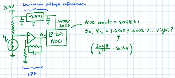 Figure 15: Does the addition of a low-pass filter in the circuit result in a 1.650±0.008 V true value? (Image source: Nathan Jones)
As crazy as it sounds, still not yet! Although this article has effectively characterized the noise in the ADC, it hasn’t yet characterized its error. After the testing outlined here, the only confidence is that two ADC values are the same or different. However, it is unknown as to whether an ADC code of 2048 corresponds to exactly 1.65 V or to something else. Gain, offset, and differential non-linearity errors (among others) could mean that converting from an ADC code to an actual voltage is more complicated than using Vin=ADC result × VFS/2N. But that’s a topic for another article!
References
Disclaimer: The opinions, beliefs, and viewpoints expressed by the various authors and/or forum participants on this website do not necessarily reflect the opinions, beliefs, and viewpoints of DigiKey or official policies of DigiKey.


